The next stage in the rover circuit project was schematic design and PCB layout. See the previous post for a wider project overview and some background research into the circuit components I implement below.
Choosing ICs
H-bridges
While I could have implemented my own H-bridge design with MOSFETs and diodes, plenty of good options already exist in IC form and have the benefit of built-in protection circuits. This board requires two full bridge circuits, each driving three motors; this allows the direction and speed of the left motors to be different from the right motors.
Initially I looked at the L293DNE which contains two full H-bridges in its single package, but later realised that it would be unable to handle the inrush current of each set of motors (up to 2A / 3 motors).
Eventually, I settled on using two DRV8876s which can each handle 3.5A through their single H-bridge.
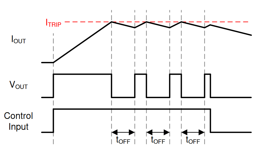
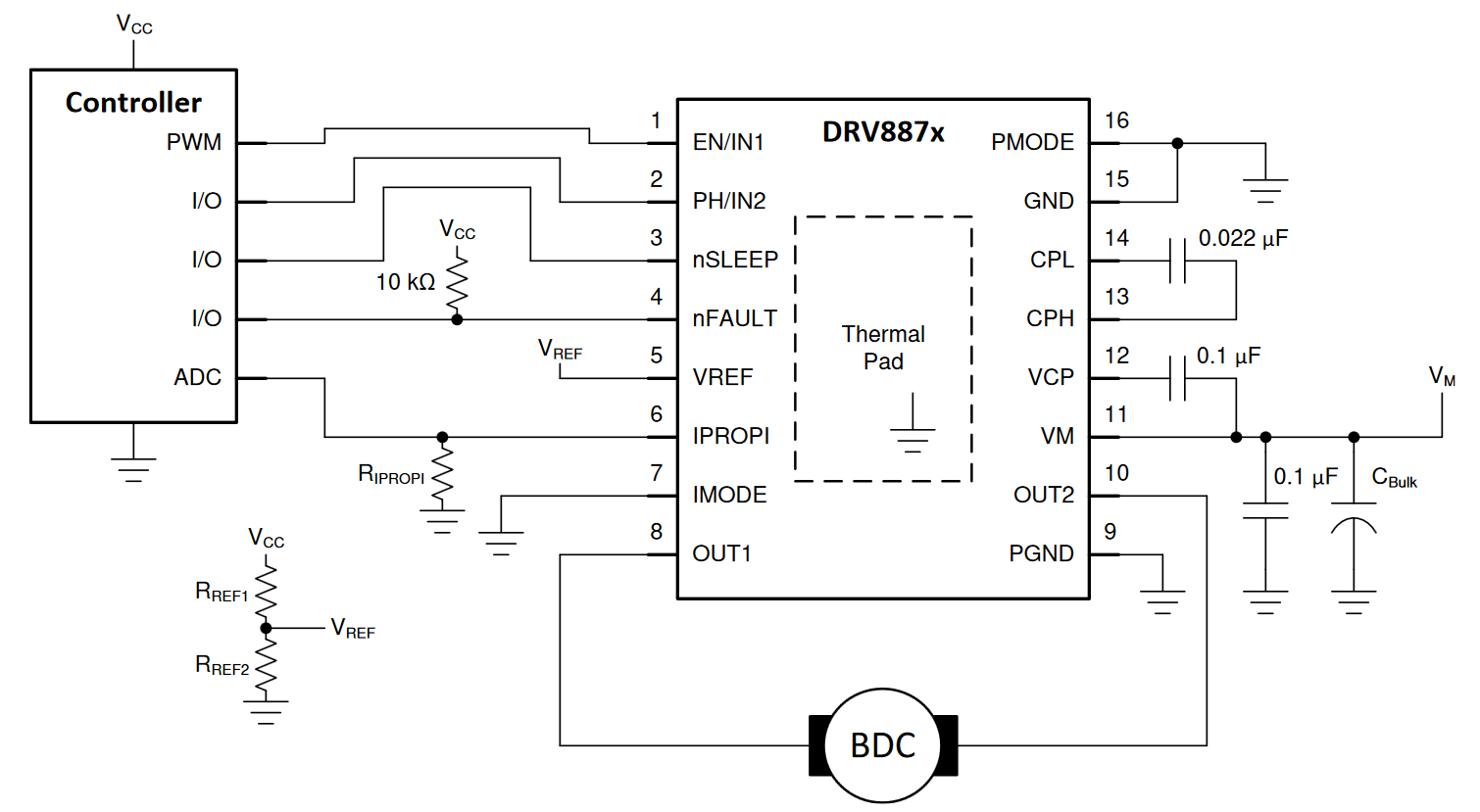
The DRV8876 also features controllable current regulation – I made use of the built-in ‘on time’ regulation which is activated on an overcurrent event. This will prevent damage to the driver if I_{out} goes above a threshold set by a reference voltage.
Each DRV8876 accepts two inputs. In PH/EN mode, a PWM enable signal controls the speed of the motors (EN) and a logic level input controls the direction (PH). This is the mode I decided to use as it minimises the number of PWM microcontroller outputs required.
The DRV8876 is only available in a surface mount package. This made soldering more difficult but meant I could make the board more compact during layout.
Buck converters
The board needed to provide the following regulated supplies from the 16.8V and 14.4V battery:
- 12V, 2A for the Xbox Kinect (used for autonomous control).
- 5V, 2A for the Raspberry Pi.
- 5V, 3A for the 4 steering servos.
- 5V for the board logic.
The motors can use the unregulated battery output so did not need a regulated supply.
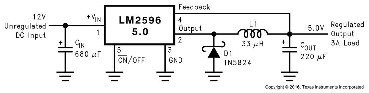
I decided to use the the LM2596 switching IC which comes in 5V 3A and 12V 3A variants. The main motivation for choosing this chip was availability as I already had some from a previous project. The LM2596 is also very simple, requiring only four external components.
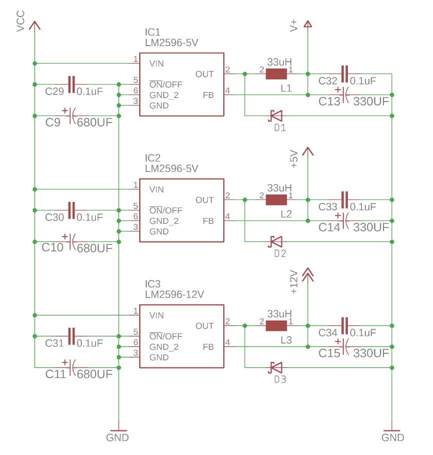
In order to ensure the 5V supply for the board logic and Raspberry Pi was clean, I decided to use two separate buck converters to create a dedicated voltage rail for each. This meant I needed to use a total of two LM2596-5s and one LM2596-12.
Microcontroller
Informed by my previous decisions, I knew the microcontroller needed to:
- Have 6 PWM capable outputs for servo control lines and motor speed control.
- Have I2C capable I/O.
- Have an ADC to measure the voltage across metal detector capacitor.
- Have a digital output for the metal detector pulses.
Based off availability and suitability I chose to use an Arduino Nano board as opposed to a standalone microcontroller. This board features the ATmega328p microcontroller along with its own 5V linear regulator and a CH340 USB to serial chip for easy programming.
Schematic Design
I did all of the schematic and PCB design in Eagle. Much of the schematic design was simply implementing datasheet suggestions and choosing components that matched the requirements laid out in datasheets.
Inductance in circuit traces means the buck supplies can take time to meet changing current demands of ICs and outputs. Wherever possible, I included local bulk and decoupling capacitors, usually 0.1µF and 100µF respectively, to quickly meet current demands. The small ceramic capacitors with low ESR would typically be first to respond to changing current demands, with the larger electrolytics providing for sustained increases.
Buck converters
These are designed in accordance with the typical application in TI’s LM2596 datasheet. The diode was picked for its short response time, important as it is constantly switching between reverse and forward conduction. The inductors are shielded to minimise interference with adjacent traces.
The capacitor values are likely larger than necessary; this was to meet the recommendations on the specification to minimise ESR (equivalent series resistance). In reality, as I placed ceramics in parallel on the inputs and outputs ESR would be lower anyway; additionally, newer capacitors have much lower ESR than when the datasheet was published.
H-bridges
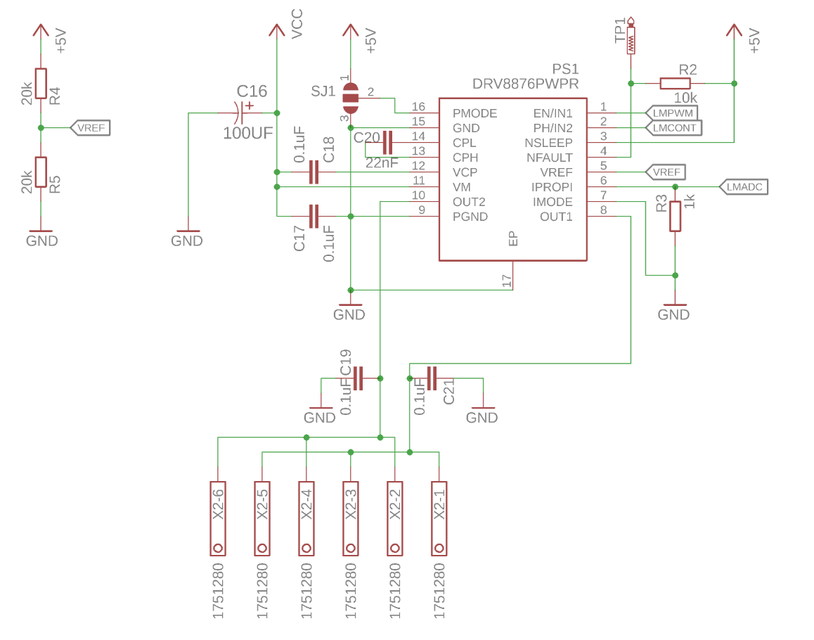
The motor drivers are permanently enabled and I added solder jumper in case I needed change their mode of operation. The chip is referenced to VREF created by a simple voltage divider from the 5V regulated output from out power supply; this is used for various internal functions including setting the maximum current to 3.4A along with R3.
Servo outputs
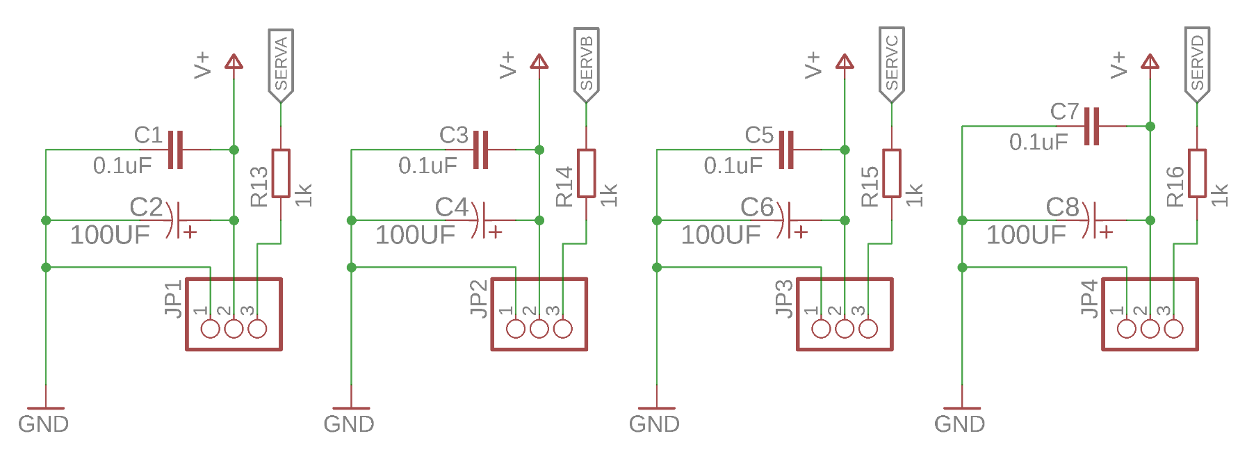
I placed a series resistor on each data line to impedance match the sender side with the receiver side. The Arduino pins can source a large amount of current but the servo data input will draw very little. A resistor on the board side will reduce initial inrush current and minimise reflections along the data line.
I also added local bulk and decoupling capacitors.
Metal detector and Arduino
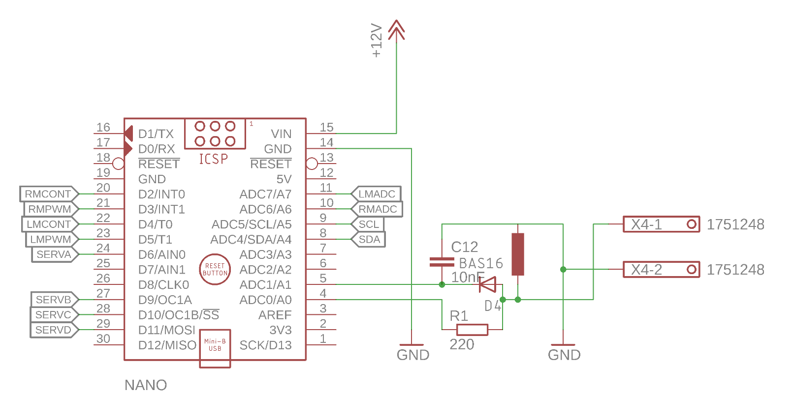
The metal detection circuit is identical to the earlier prototype. I decided to use screw terminals, allowing the detector coil to be attached and taken out as required. A0 provides the pulses and A1 measures the p.d. across C12.
The Arduino is powered from the regulated 12V supply; its own on-board regulator steps this down to 5V. Most unused inputs are left floating.
I/O
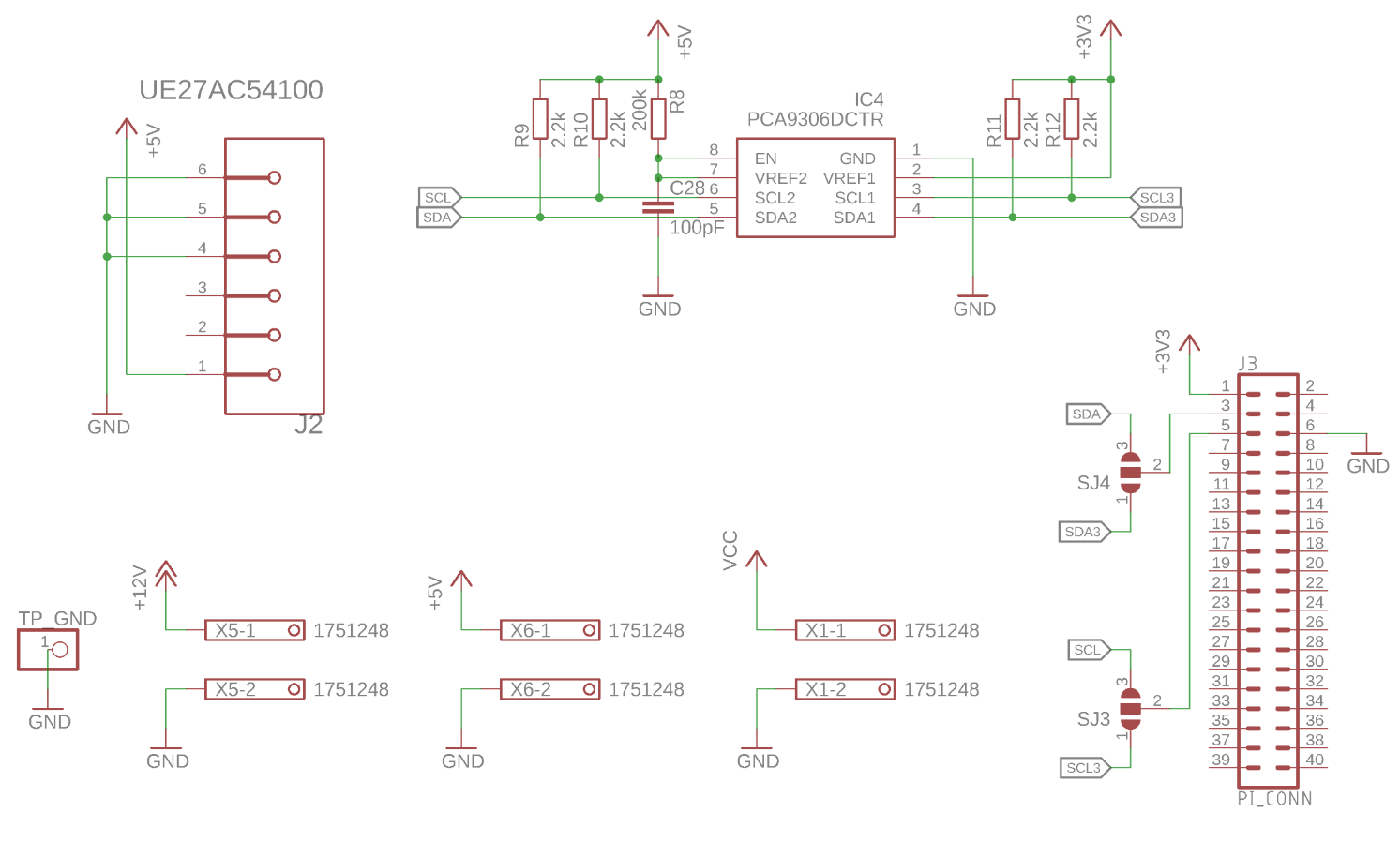
The board provides a power output for the Kinect and an additional 5V output.
All of the Pi GPIOs plug into the board via a ribbon cable but only those required are connected. The Pi is powered through a separate USB port on the board, this is safer than supplying power through the pin header as it does not bypass protection circuitry.
The most complex part of this circuit section is the PCA9306 which is a bi-directional I2C logic level translator. This steps up/down the I2C communications from the 3.3V Pi and the 5V Arduino.
PCB Layout
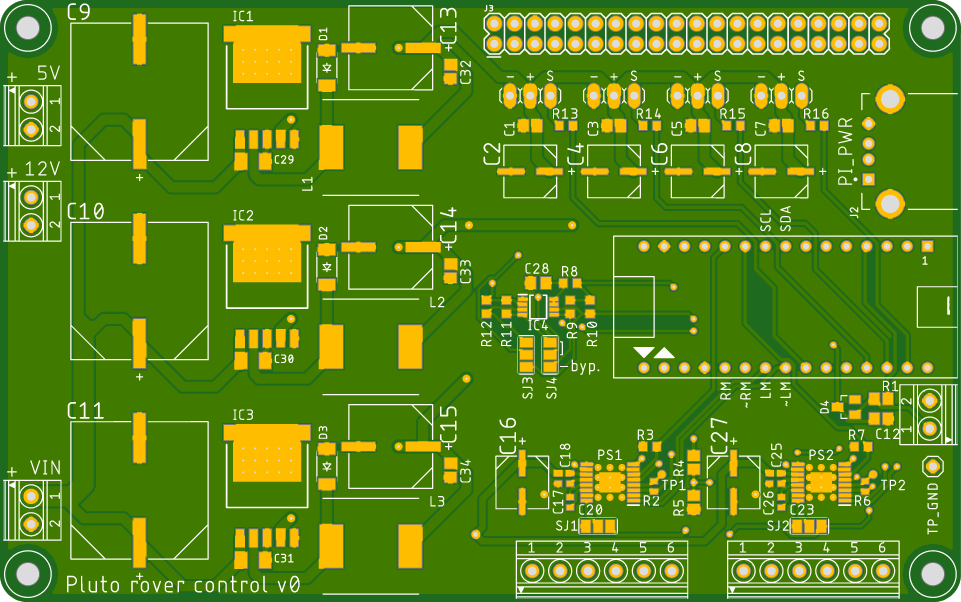
Once I had the schematics finished I moved on to the PCB layout. To ensure the board would not take up too much space I used SMT (surface mount technology) components wherever possible; this also gave me access to more modern ICs such as the motor drivers. Most capacitors and resistors were size ‘0402’ (1mm × 0.5mm).
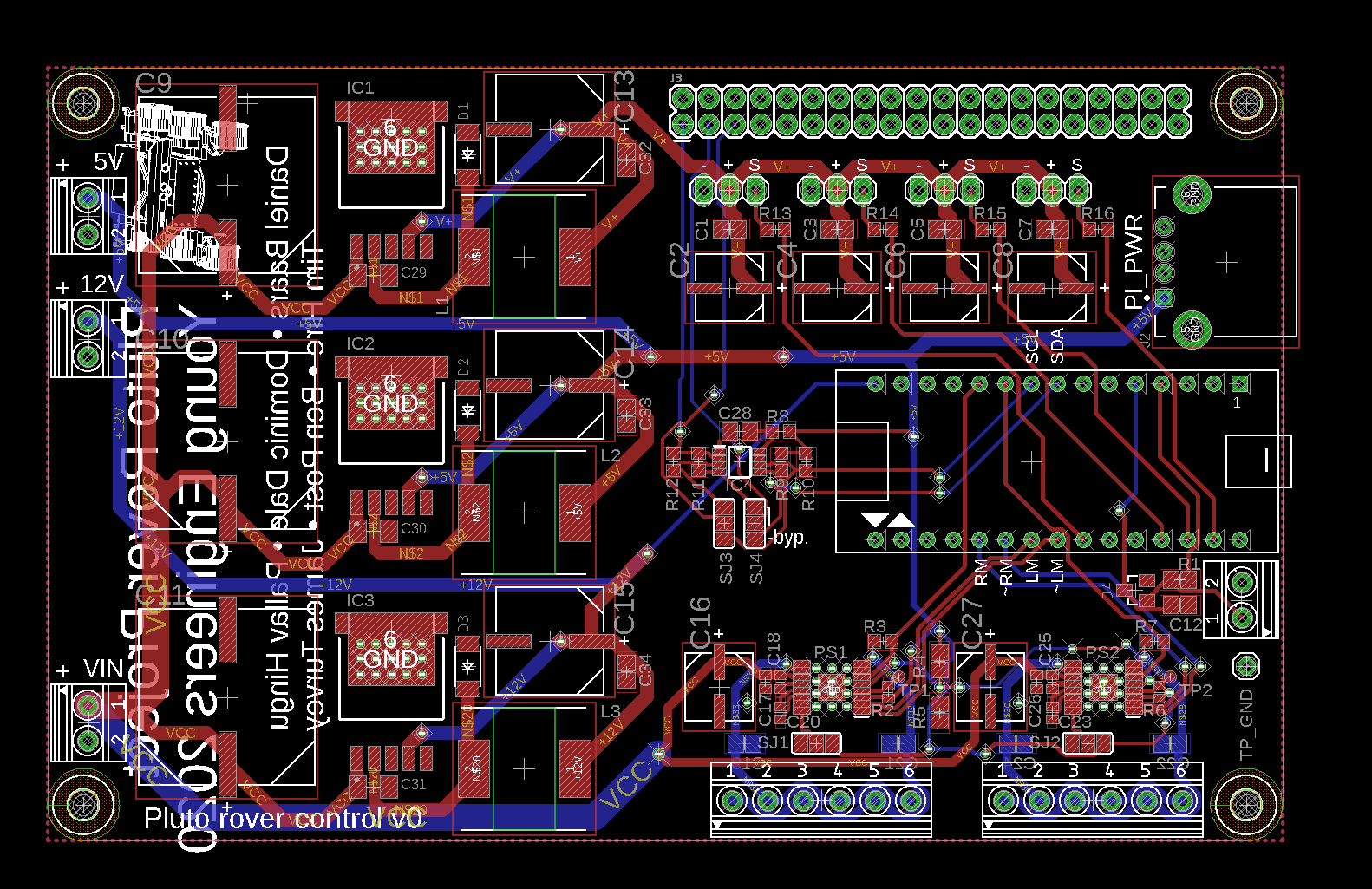
I laid out the largest sections of the circuit first, starting with the buck converters. It was important that I/O was accessible, especially considering the cramped chassis, so I placed all screw terminals around the edges and ensured all ports had sufficient mechanical clearance.
During layout I tried to stick to PCB design best practices. IPC-2221 recommendations were used to determine trace width based on the current through each trace. Furthermore, all capacitors were placed as close as possible to the loads they supply.
Both sides of the board feature ground fills which means any copper areas left after components and traces have been placed are electrically connected to ground. This is extremely useful as most components connect to ground and a fill makes it accessible across the board. Additionally, the ground fill can act as a heat-sink – both the motor drivers and buck converters have thermal vias that transfer heat to the other side of the board where it is dissipated through the large copper area.
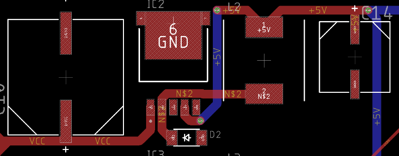
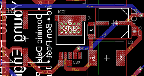
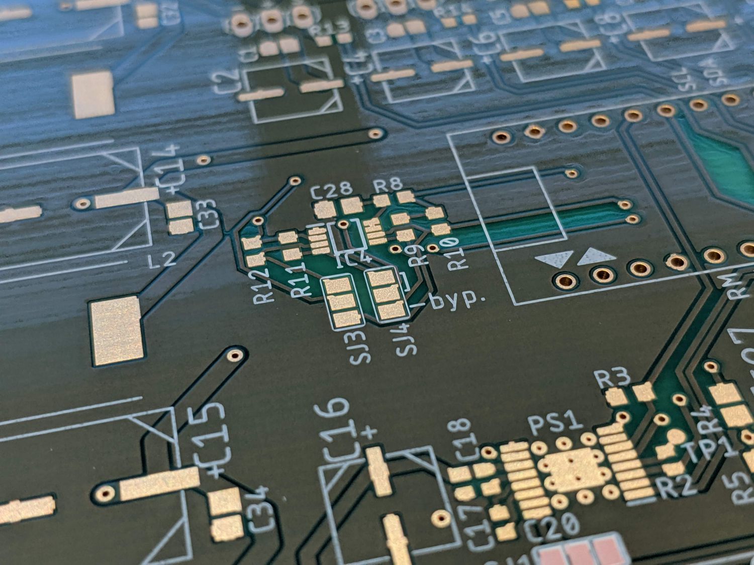
Following feedback from an electrical engineer who specialises in power supplies, I rearranged the buck circuit to minimise the loop when the diode is in reverse conduction. Additional ceramic smoothing capacitors were also included and the feedback line was rerouted to reduce noise. A comparison of the two designs is shown above.
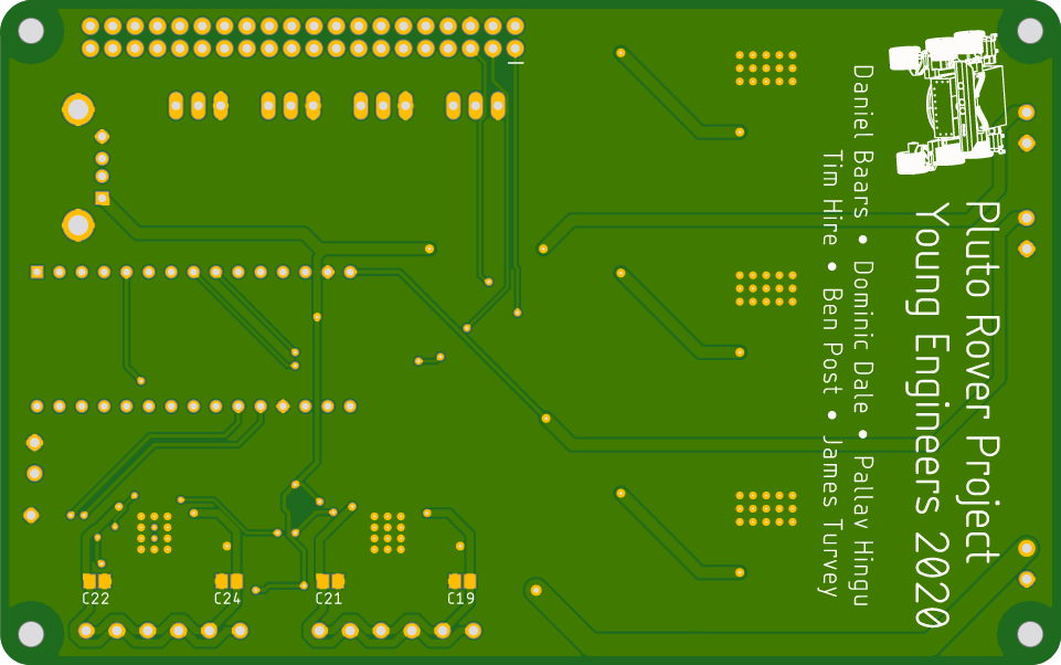
Finally, I added some decorative silkscreen on the back and sent the board off for manufacture.
Conclusion
The board schematics and layout were an immense amount of work but I am extremely pleased with the outcome, and it was a lot of fun to make. To finish the circuit I needed to solder the board together, which was my first attempt at SMT assembly, and test the completed board. See that process here.