This summer, I worked as a firmware placement student at a large UK engineering firm. My focus was learning to use MATLAB’s firmware development packages in Simulink to implement signal processing on a software defined radio (SDR). This was a steep but rewarding learning curve given this was my first introduction to firmware development. I’ve documented a high level summary of what I worked on and learned below. In contrast to some of my other posts, this article is likely to be text-heavy and a bit general in some areas to avoid breaching confidentiality!
Rather than working within an existing product team, our cohort, made up of current university students, was assigned our own project to deliver over the course of just 8 weeks. Each of us were given rough roles, from systems to software, based on our past experience, with the aim being we would get a chance to experience all disciplines in the engineering process of the product.
The brief required a pulse detection solution for signals in the microwave frequency range to be developed. The client already possessed hardware capable of processing signals in the 70MHz-6GHz range but wanted an extension in the usable band to detect 20-60GHz signals. This meant four key technical areas were required:
- Antenna design to receive all required frequencies in this band.
- Microwave design to down-convert high frequency microwaves to lower frequencies that the existing hardware could detect.
- Firmware development to implement digital real-time processing on the received signals.
- Software development to provide final stage interface with and delivery to the user.
Ambitious for a set of untried undergraduate students you might think! – but fortunately subject matter experts in each field, themselves working on other projects, were on hand to advise.
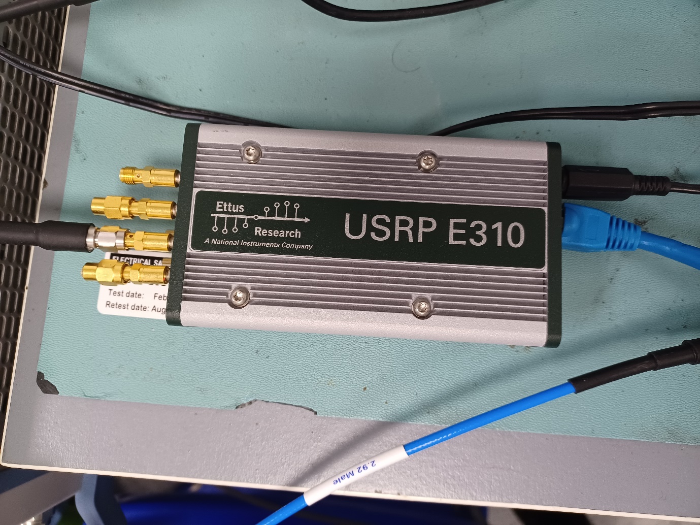
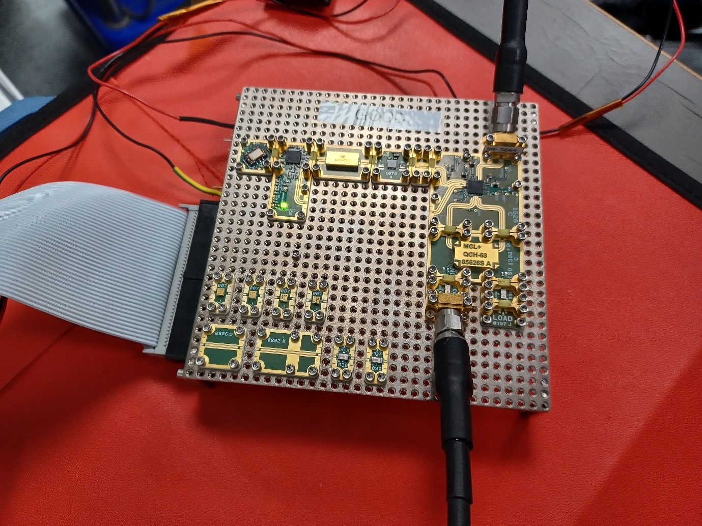
The main pre-specified processing hardware was an Ettus E310 software defined radio (SDR). A traditional radio chain uses hardware to provide mixing, filtering and amplification; this might be done digitally on ICs or with fully analogue components. SDRs are becoming increasingly popular because they allow full software configuration to replace these sorts of components. Received signals are immediately down-converted and fed into high resolution ADCs for processing with FPGAs and/or MCUs. Signals can also be generated or processed for transmission.
Field Programmable Gate Arrays
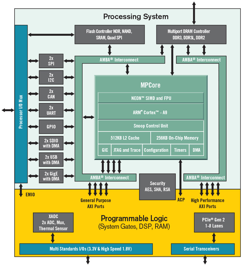
As one of the two firmware engineers, my role was FPGA firmware development. An FPGA (Field Programmable Gate Array) is an IC based around a set of configurable logic blocks that can be set by firmware to perform different tasks – interconnects between these blocks are also set. The E310 features a Xilinx Zynq-7020 which integrates an ARM-based processor with an FPGA.
Microprocessors execute one instruction per cycle, so are unsuitable for high throughput applications such as real-time processing of high resolution signals. In contrast, after setting an FPGA’s gates, it can process signals almost as fast as they enter, only slowed by the propagation delay of the programmed logic which is typically far lower than the clock speed of the device.
Instead of a programming language, firmware design for FPGAs is done with a hardware description language, in this case VHDL. HDLs are used to describe the behaviour of digital logic circuits: the same HDL used to set an FPGA’s gates could eventually be used to create masks for a dedicated IC.
Something of particular interest to me was the clear high-level parallels between PCB development and firmware development:
- HDL is synthesised into a netlist, simply made up of nodes and their connections within the FPGA.
- The netlist is then implemented by placing and routing the nodes for writing to a physical device.
Thankfully, for HDL developed firmware and hardware, leaving implementation to the autorouter is the best and only option. Dealing with 62222 nets manually would be unlikely to end well.
Typical firmware implementations in a signal detection chain
The first step in developing our firmware solution was deciding on what exactly we wanted it to do. In the E310, ADCs at the input feed the digitised antenna signal onto a bus accessible by the FPGA; we needed to take this data, do some processing and pass on useful information about incoming pulses to the processor.
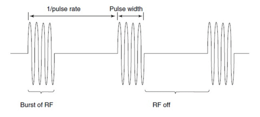
But what exactly does an RF pulse look like? For our scenario we assumed that any pulse would be amplitude modulated and at constant frequency. We might detect a few milliseconds of high power at a given frequency followed by a lower power or no signal at that frequency thus indicating a pulse. The maximum frequency at which pulses can be sent (i.e. the data throughput if this were a transmission line) is much lower than our 20-60GHz carrier frequency.
In industry, FPGAs are often configured to generate pulse descriptor words, or PDWs for short. These contain information about detected pulses like frequency, pulse length, time of arrival and duty cycle; the processing to find these characteristics is all done with minimal latency on the chip. PDWs can then be sent to an external computer to alert an operator or be logged in a database.
If this were a defensive system, the FPGA might be configured to take immediate action, for example by transmitting a response signal to mislead any adversaries.
The systems engineers on our team decided generation of PDWs was the best role for the FPGA to fill.
Our model based approach
Sadly, 8 weeks would be far too short a time to learn how to implement a full PDW generation system in HDL. Thankfully, there was a solution: Simulink’s firmware development libraries.
Simulink is a block diagram based modelling environment which makes it easy to put together systems with defined inputs and outputs. These systems can then be simulated with testbenches also made in Simulink, and data on any buses can be monitored for debugging.
Before the placement began I didn’t have any experience with MATLAB or Simulink, but with some practice it was easy to see why it’s so widely used. The simulation and monitoring tools are excellent and manipulating large matrices at different data rates is all fairly intuitive. The HDL extensions compile Simulink blocks down to VHDL or Verilog for standard synthesis and implementation on an FPGA – they also support Xilinx’s processing system natively meaning the software interface running on the ARM processor can also be fully programmed from Simulink.
Within a short timescale we were able to get a Fourier transform peak finder running on the SDR and began working towards full pulse identification and storage. This was a really interesting and unique introduction to firmware development, and I’m glad I was able to experience every stage of the development process.
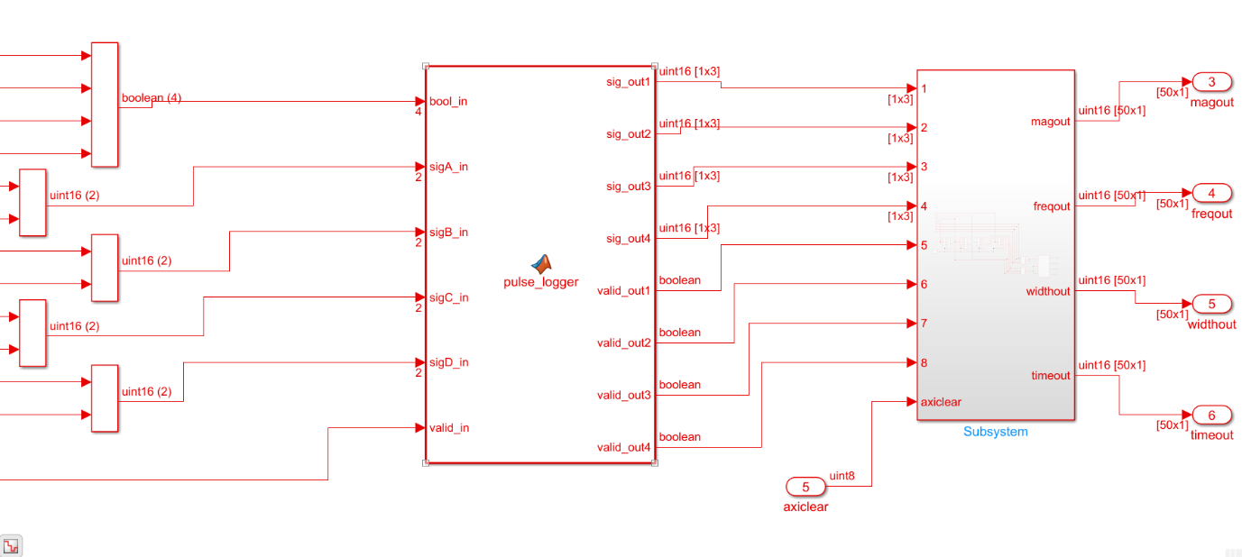
A full breakdown of our PDW generation model is shown below:
- The FFT: Transforms incoming signal into frequency domain, bins of defined frequency range each with a magnitude generated.
- Peak finder: Finds the bins with greatest magnitude.
- Pulse identification: Identifies if any of these peaks are pulses above our threshold value.
- Pulse logging: Logs each time a pulse is seen for pulse width calculation.
- PDW generation: generates the final descriptor package for immediate transmission.
Parallel experimentation with VHDL
I didn’t want to completely neglect the traditional approach of writing firmware, and thankfully, in parallel to the main project, I was given an introductory project to do on a Nexys A7 FPGA board.
Similar to Simulink development, VHDL is versatile in that it can be used to define the logic of a system, while also defining a test-bench around it. Only a subset of VHDL is actually synthesisable – typically that at the Register Transfer Level (RTL). This describes VHDL at its lowest level of abstraction where instructions are usually configuring individual registers and look-up-tables.
Understanding the file-structure of VHDL projects was a hurdle in itself to overcome but with a lot of fiddling I was able to get an LED blinking! Simulation played a key role in this endeavour with timing issues causing me particular headaches – searching through binary signals on output pins is a bit more painful than using Simulink’s various tracing tools.
I’m glad I was able to have a taste of this side of firmware, especially given its still the main way the company I was at developed for its products. Learning about VHDL functionality also explains why a lot of the Simulink generation is structured in the way it is.
Synthesis and implementation
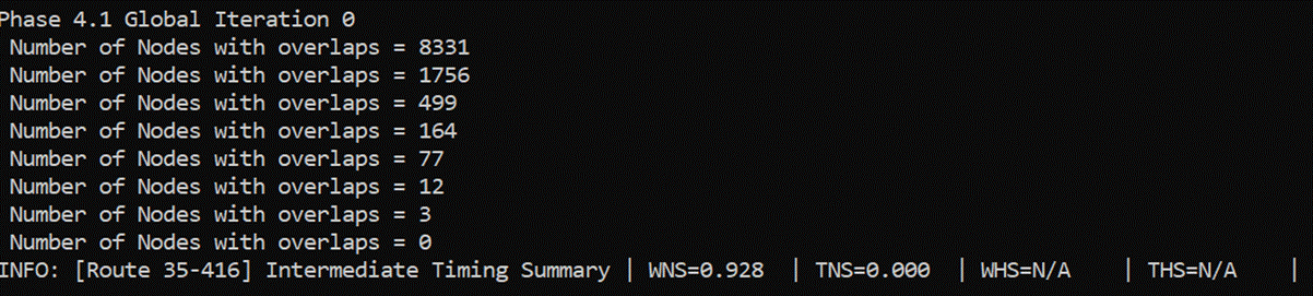
With our model perfectly working in simulation and compiling to VHDL, the final two stages were synthesis and implementation. This is where we ran into some of the toughest problems including timing errors and space constraints; but with a bit of perseverance we were able to get our model running on the board.
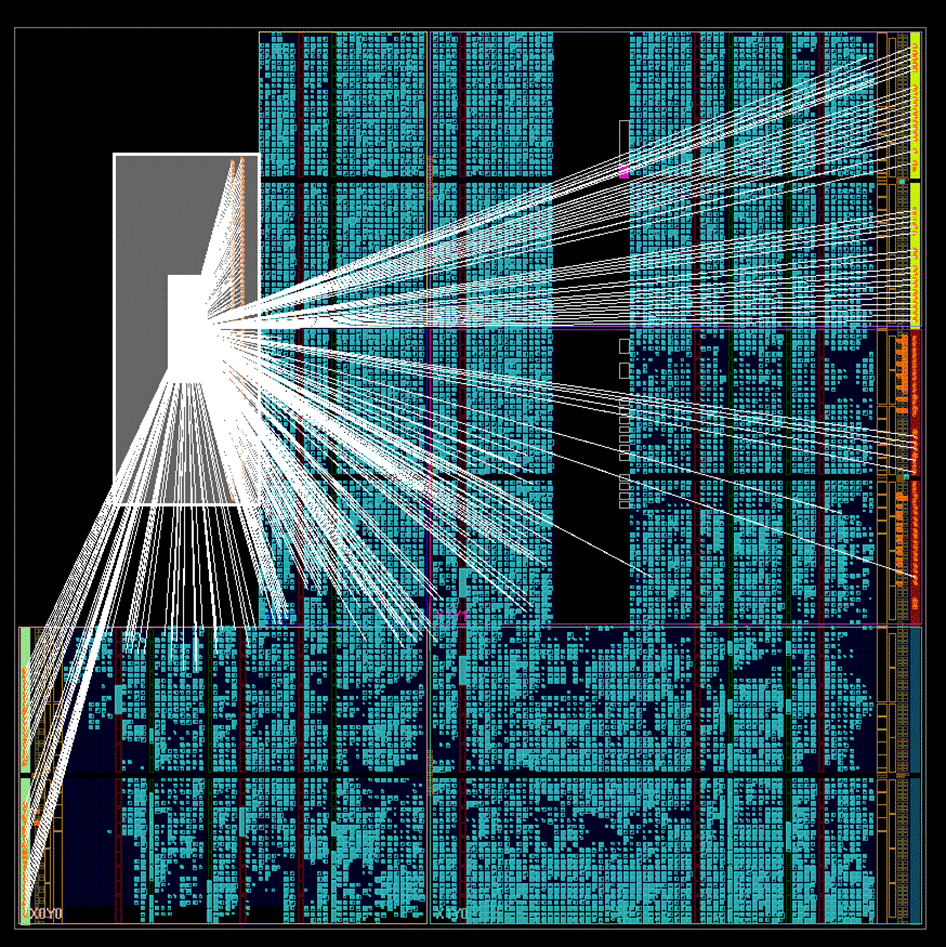
Vivado is Xilinx’s software for both tasks and for the most part was straightforward to use and helpful in flagging up what was causing issues. It includes impressive graphical tools for visualising the FPGA layout and interconnects: below you can see all the connections to the PS (processing system) IP wrapper after layout.
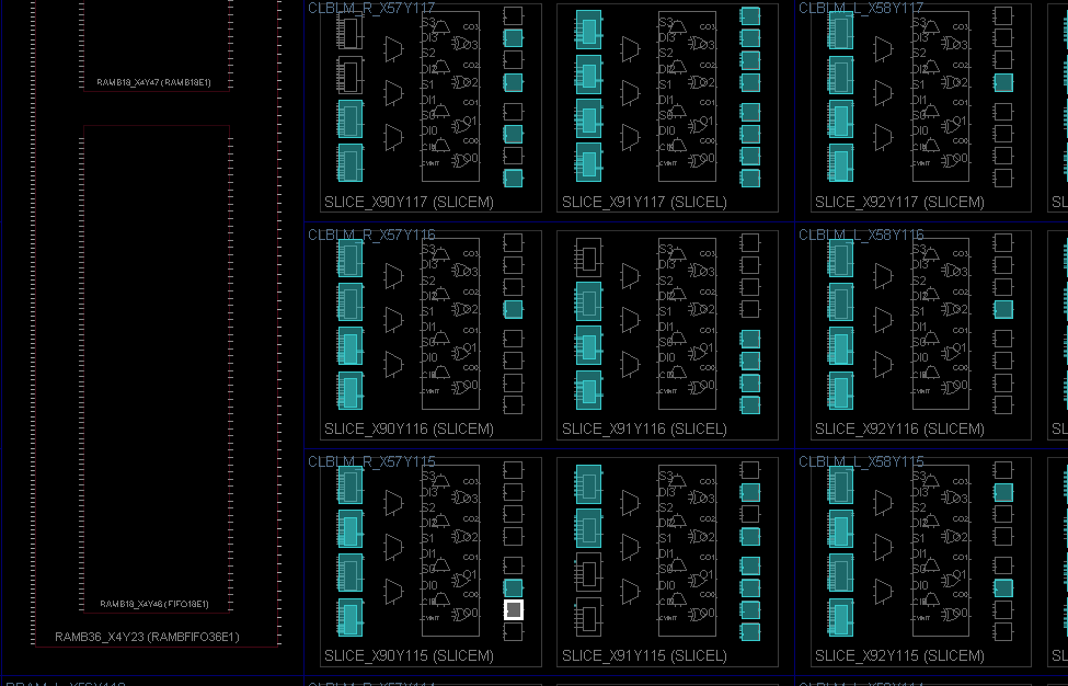
When you zoom in, you can see the core logical elements of the FPGA. LUTs (lookup tables), flip flops, multiplexers and carry chains are organised into thousands of slices. RAM, I/O and other specialised logic exist elsewhere on the chip.
When running implementation, Vivado is finding the best physical way to connect all of these different logical elements. This generates a bitstream which is transferred to flash storage on the device; every power cycle Xilinx’s PS loads this configuration into the gates of the FPGA.
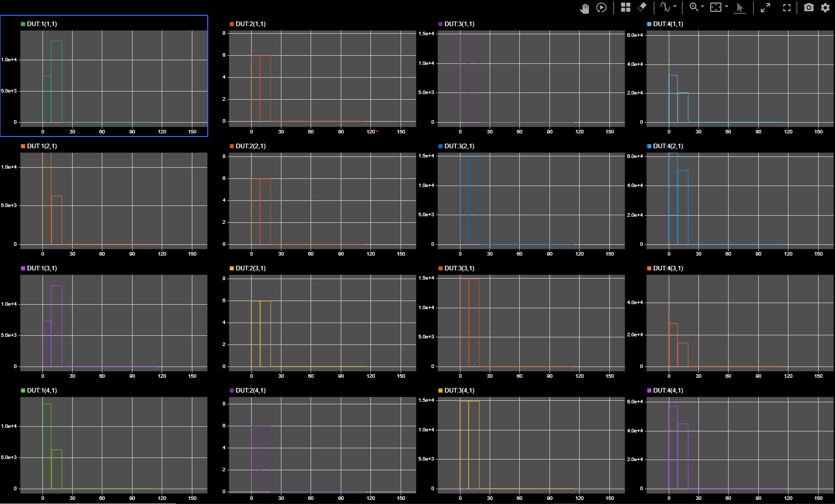
With a firmware bitstream on the device, the testing stage could begin. Not only does Simulink support firmware development for the Xilinx 7020 series, but software to run on its processing system can also be created and run with real-time logging – ideal for finding issues. One of our testing interfaces is shown below with four PDWs displayed.
In the end we did manage to get full PDW generation capability working within the RF chain.
Conclusion
Having had no former experience of firmware development, this placement was a fantastic chance to approach it from two different angles and I’ve learned a huge amount in the process. Study in this area is something I hope to continue and I may try to incorporate FPGAs into future personal projects.
Working in an engineering firm is a very different environment to university, and while the change was a shock, being able to switch off after 5pm is something I’ll certainly miss as I go back up to Selwyn. I’ve begun to appreciate that an engineer’s remit is far greater than just technical expertise; communications skills and team working ability are of equal importance and being able to develop these was another highlight of the last eight weeks.