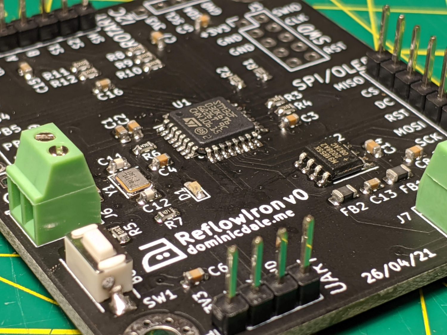
Recently I moved from Eagle to KiCad EDA and one thing I missed was the ability to use Fusion 360’s rendering workspace. KiCad has its own 3D viewer with rendering included but it is fairly limited.
In this article, I’m going to go through my process of generating fairly realistic renders in Fusion 360 from PCB designs originating in KiCAD.
Assigning 3D models
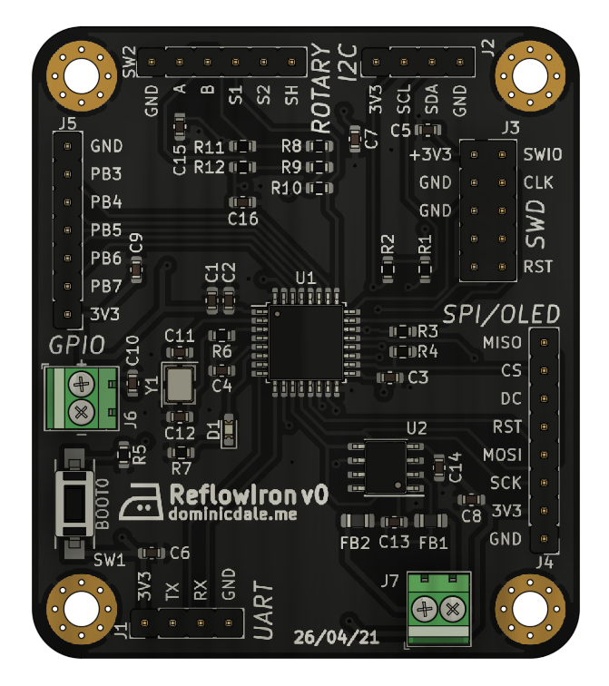
The first step is ensuring all components on the board have assigned 3D models. By opening the 3D viewer with ALT + 3 you can quickly check which footprints are populated and which need their models updated.
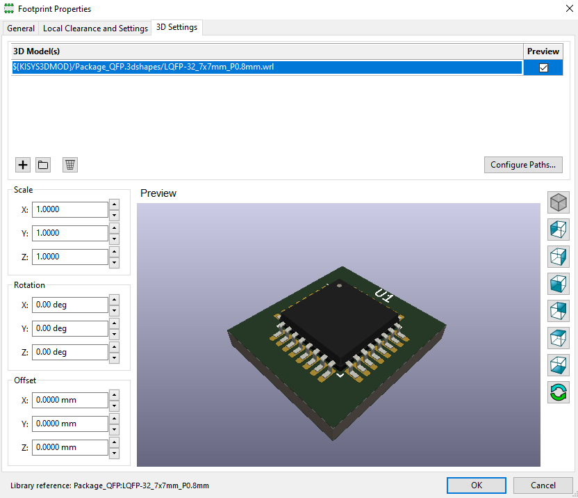
The 3D model configuration for individual components can be accessed by hovering over a component, pressing E and navigating to the 3D settings tab.
Here, multiple 3D models (both wrl and step formats are supported) can be added. In most cases, no configuration will be necessary as almost all of the default footprints come with associated 3D models. KiCad automatically selects models of the same package and name from the 3D model directory registered under “Configure Paths”. Additional models can be added from anywhere on your computer but it makes sense to do this from somewhere permanent (e.g. the project folder).
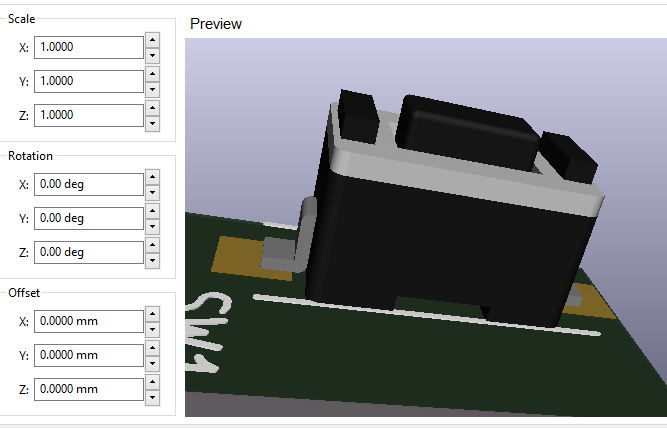
When trying to find 3D models for empty footprints I tend to check manufacturer websites, who often provide mechanical CAD files free of charge. Alternatively, GrabCAD has a huge library of free 3D models including for many electronic components. You can scale, rotate and translate the models from within the properties window to ensure they properly match the footprint of the component.
KiCad rendering
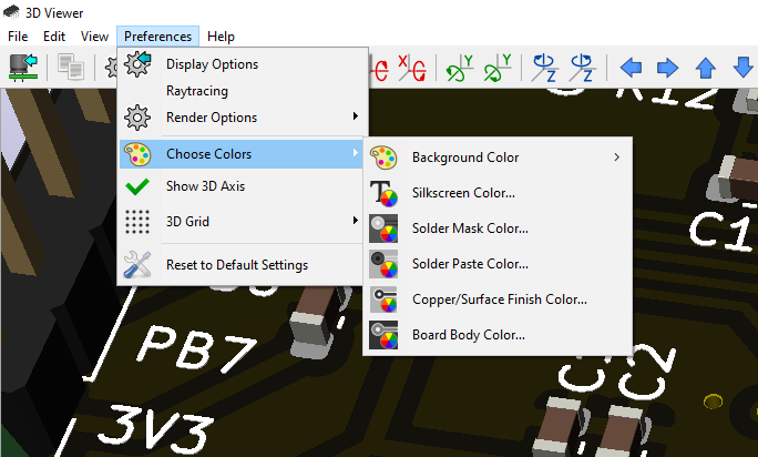
With the 3D models picked, you can immediately take advantage of the built-in previewing and ray tracing in the 3D viewer.
The ‘preview’ rendering is OpenGL powered and reasonably fast, which makes it useful for checking the looks of your board at regular intervals. You can enable raytracing in the top bar; this gives much more photorealistic results at the expense of rendering speed.
The viewer has limited customisation options but key features such as changing the solder-mask and background colours are available.
For more options, including finer material property control and ability to place the PCB in a wider design, the 3D model can be exported into Fusion 360.
Fusion 360 rendering
Exporting (and importing) the 3D model
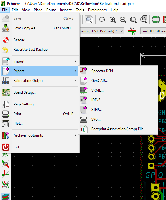
A STEP format 3D model of the entire PCB assembly can be exported directly from the Pcbnew export menu. This file can then be uploaded to a project in Fusion 360 where it will automatically be converted into an editable file.
The colours of the PCB components are preserved but graphics of the actual traces/surface finish are lost: instead the FR4 is all just a green hue.
Via holes are also lost on export though I didn’t find that this affected the look of the final renders. If required, these could be added back in by plotting them to a DXF and importing them into Fusion 360.
Adding PCB graphics
In order to add copper/silkscreen/soldermask graphics onto the board, we need images of what the final board will look like after manufacture. We can then add these images to appearances in Fusion 360. These are the sort of images you might see when uploading your board to a fabrication house in the preview window.
After trying out a few programs and plugins, I have found the easiest way to obtain such images is by using the open source tracespace tools. These create beautiful renders of gerber files automatically, from identifying which layers mean what based on their names, to generating and exporting the images based on fully customisable configurations.

Tracespace outputs vector images which need to be rasterised so they can be used as a Fusion 360 appearance. To do this I use Inkscape.
The method I outline below is all done through the command line for easy repeatability, though it may be faster to use the graphical tools if you just want to generate one render. Tracespace has an online version at https://tracespace.io/view/ and Inkscape is installed with both a command line and graphical interface.
Plotting suitable gerbers and drill files
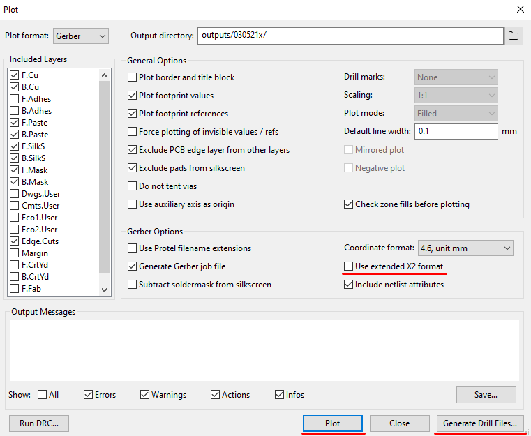
To export gerber files from KiCAD you use the ‘Plot’ window (accessible under ‘File’). In my experience, using the extended X2 format can cause issues with tracespace, so I disable it. I also disabled via tenting.
Clicking ‘Plot’ will actually export the gerbers and the drill files need to be generated separately with the marked button.
Generating the images using tracespace-cli
You can install the tracespace-cli globally with node package manager:
npm install -g @tracespace/cliThen, to actually generate the graphics you use the tracespace command. This command can take configuration options as parameters, or alternatively it will search the working directory for a .tracespacerc config file.
My .tracespacerc configuration file contained the following for this project:
The input here is a directory containing all the gerbers and drill files. To indicate this, the command must be entered as below:
tracespace -L -o "/path/to/output/" "/path/to/input/*.*"The -L flag means the program will only generate graphics for the top and bottom layers, not each individual layer. With that done, I now have two .svg files, one for each side of the board.
Rasterising the vectors
The vectors can be rasterised with the Inkscape command:
inkscape -d <dpi> -e "/file/to/output.png" "/file/to/input.svg"I’ve found that a DPI of 600 works well (though less may be acceptable).
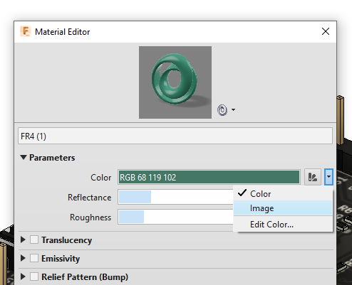
Adding the images to faces
With the two graphics prepared you can now move over to Fusion 360 and open the appearance window in the PCB model. Each face will require its own material – you can create these by duplicating the included FR4 material and changing them to images as below.
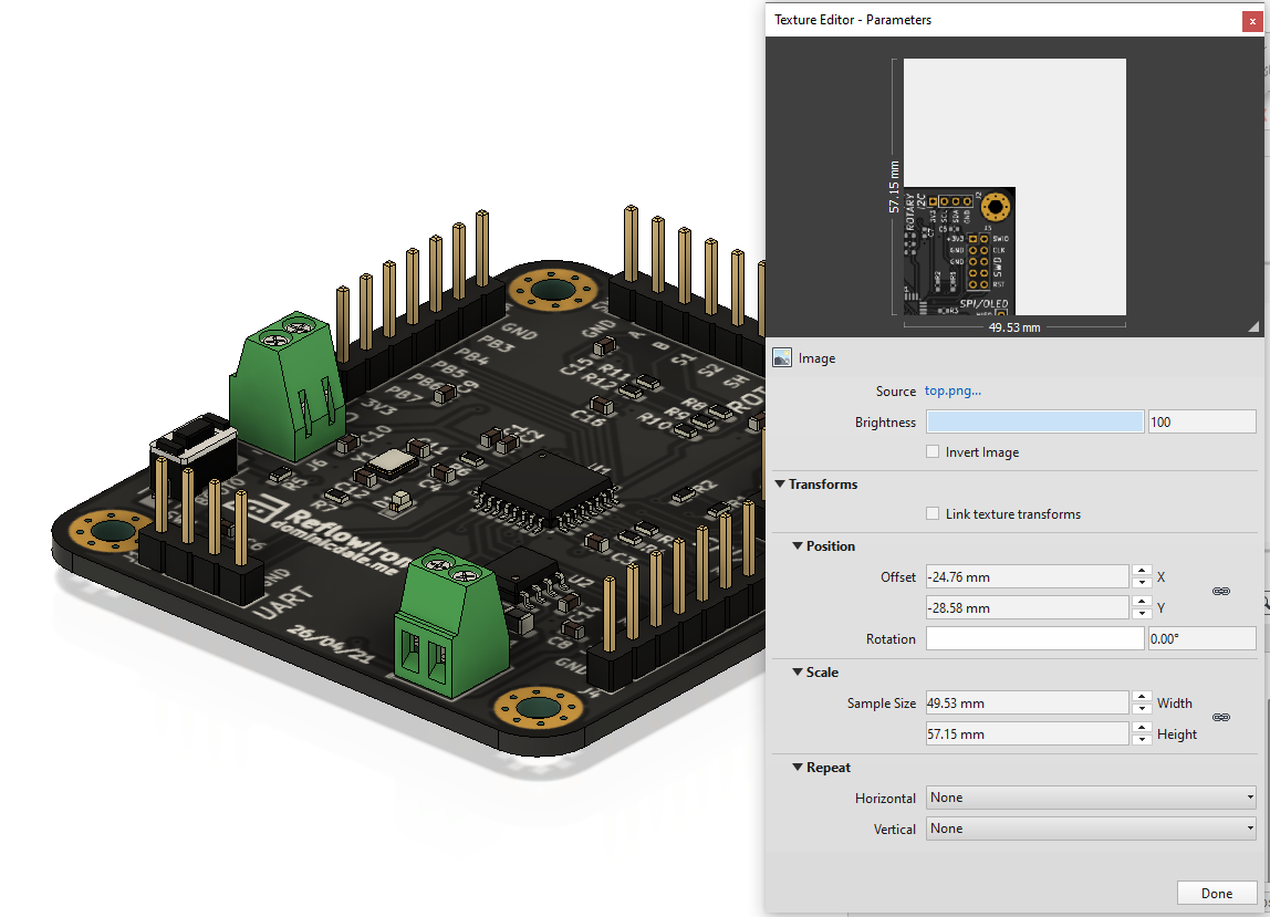
Once the image of the material is selected, set the sample size to the dimensions of the PCB; this ensures the scale is correct. Finally using the offset values move the texture so it lines up with the physical board below. The offset is usually around -½ * the length of the PCB along that axis.
To ensure any through holes and the edges fit in, you can use a third material set to the colour of the soldermask/surface finish.
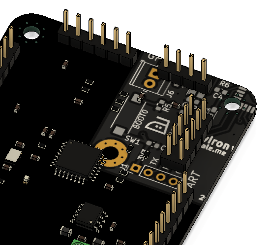
Rendering
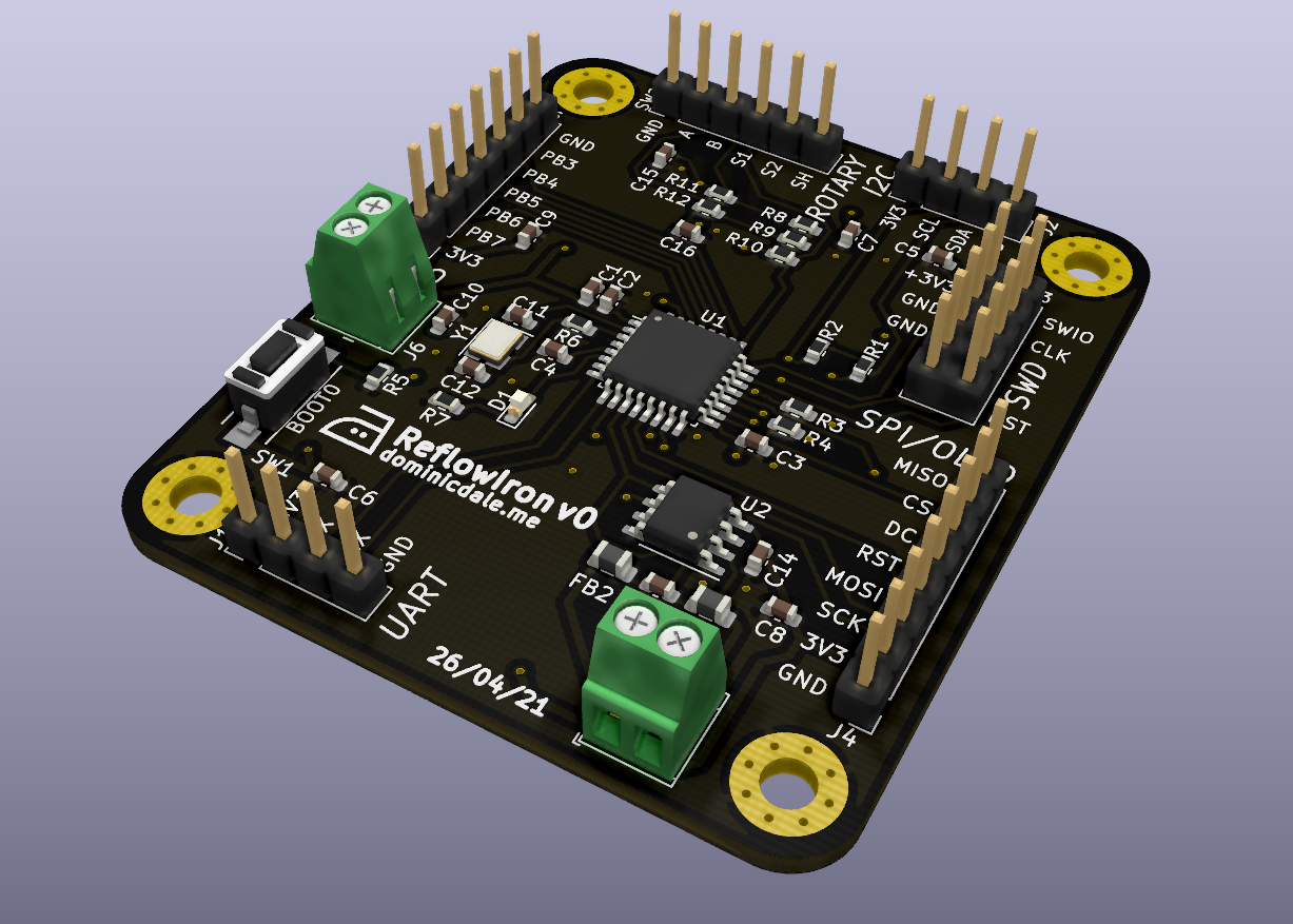
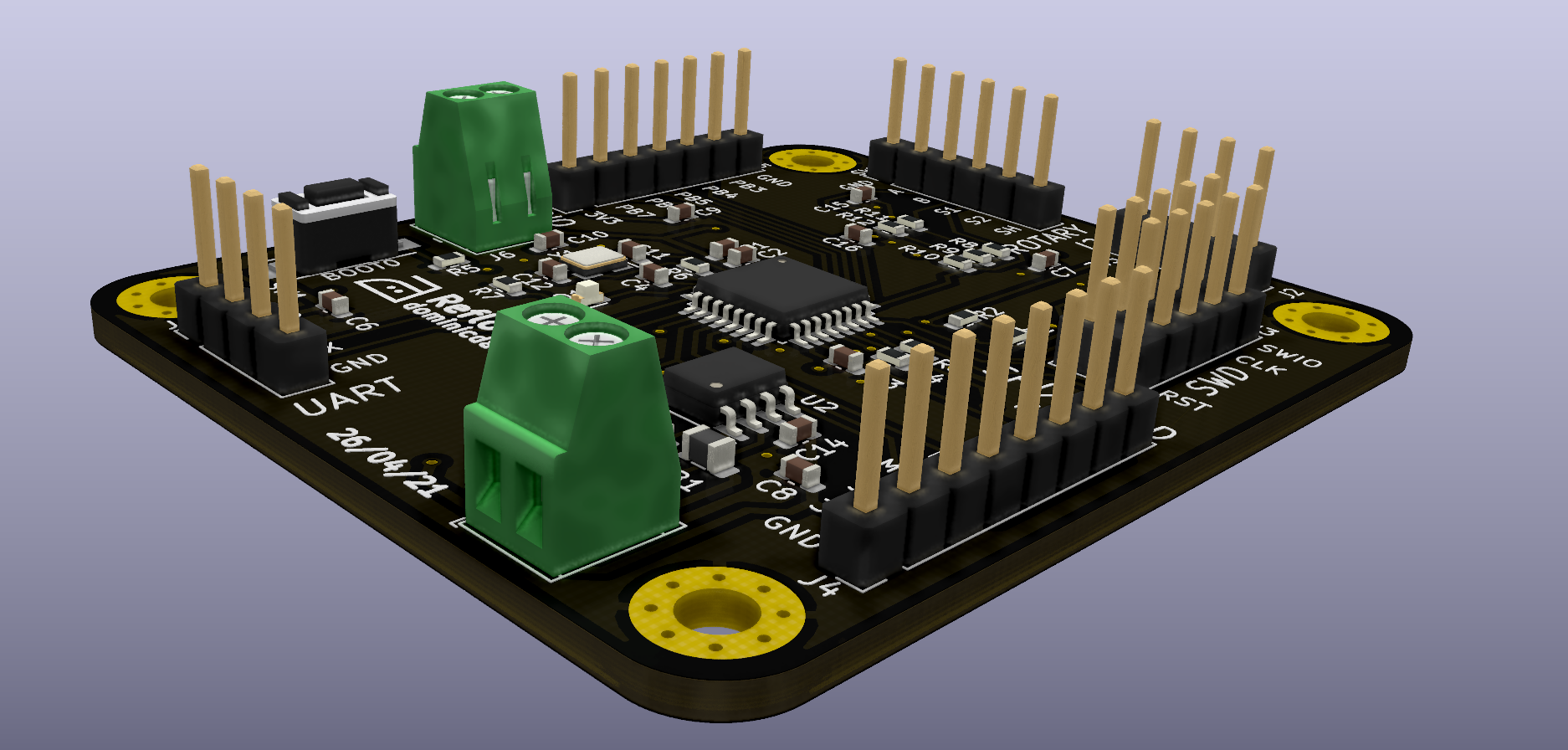
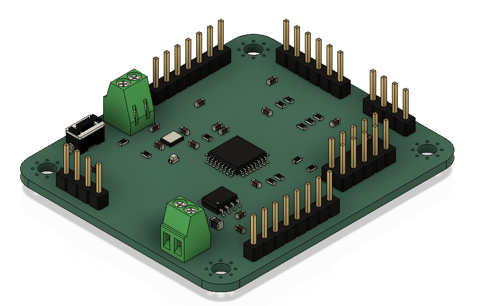
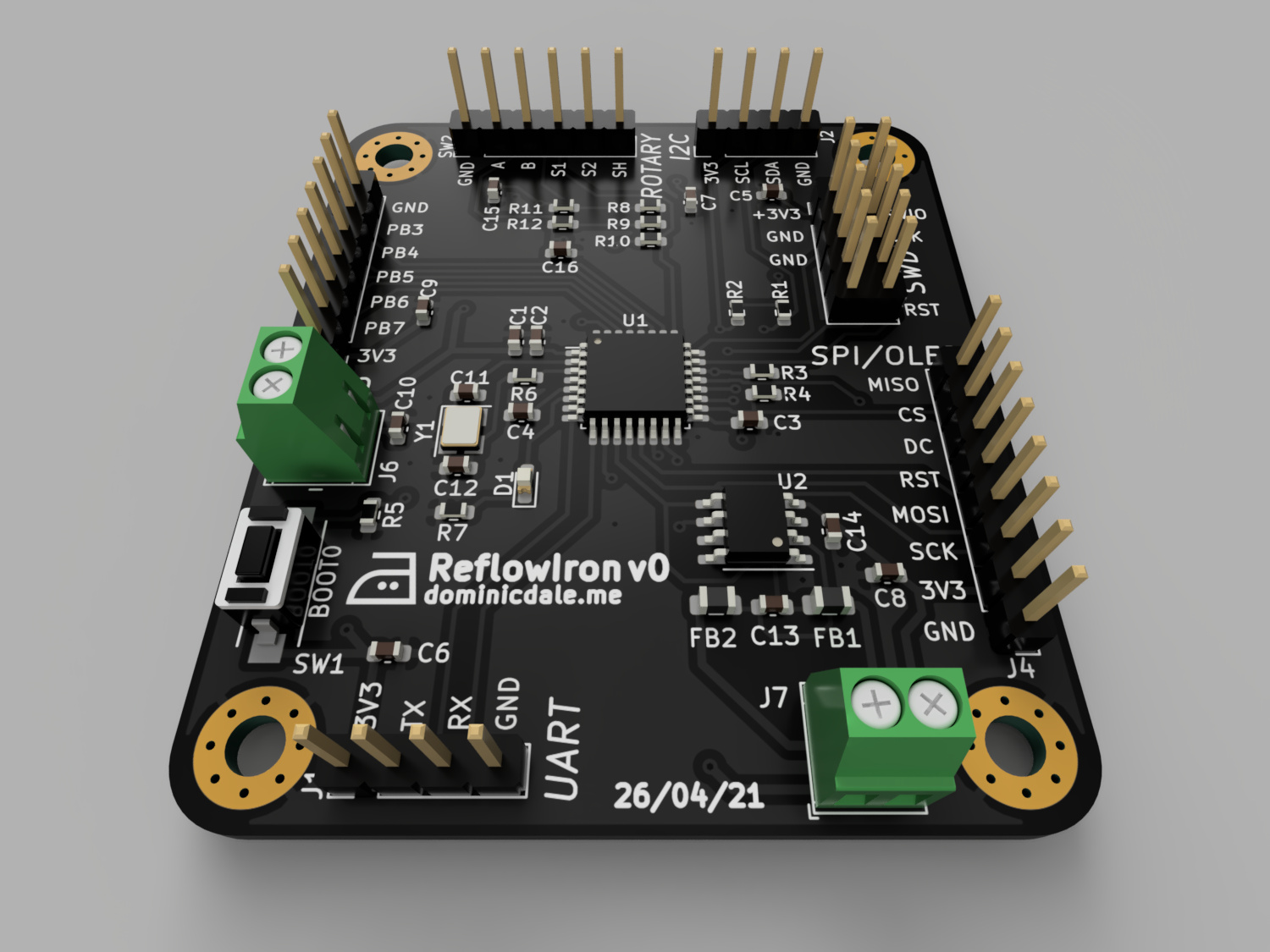
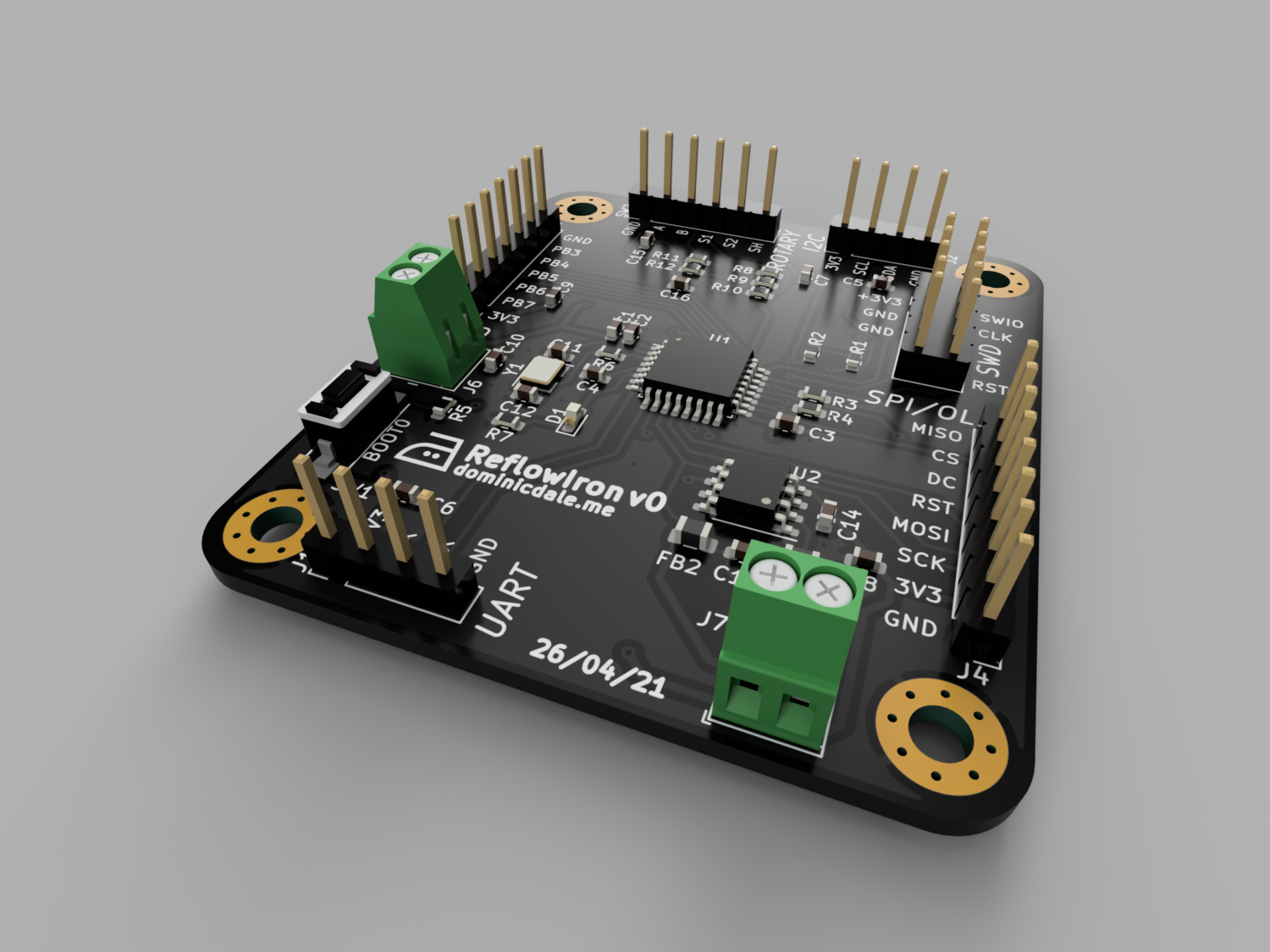
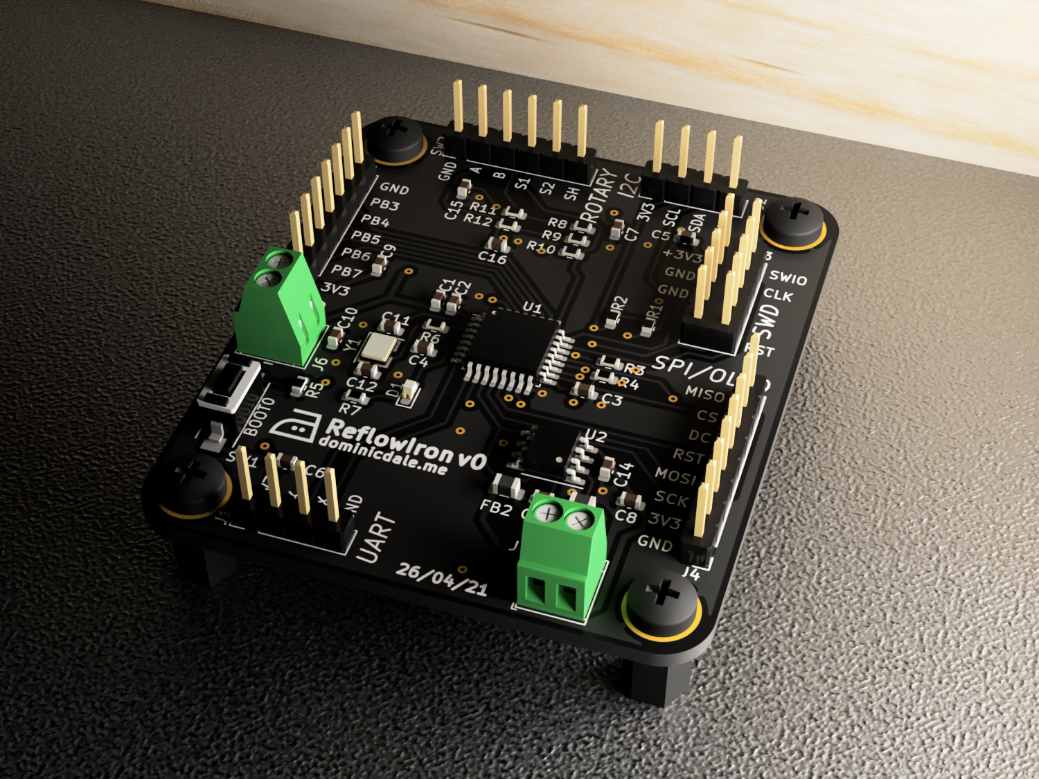
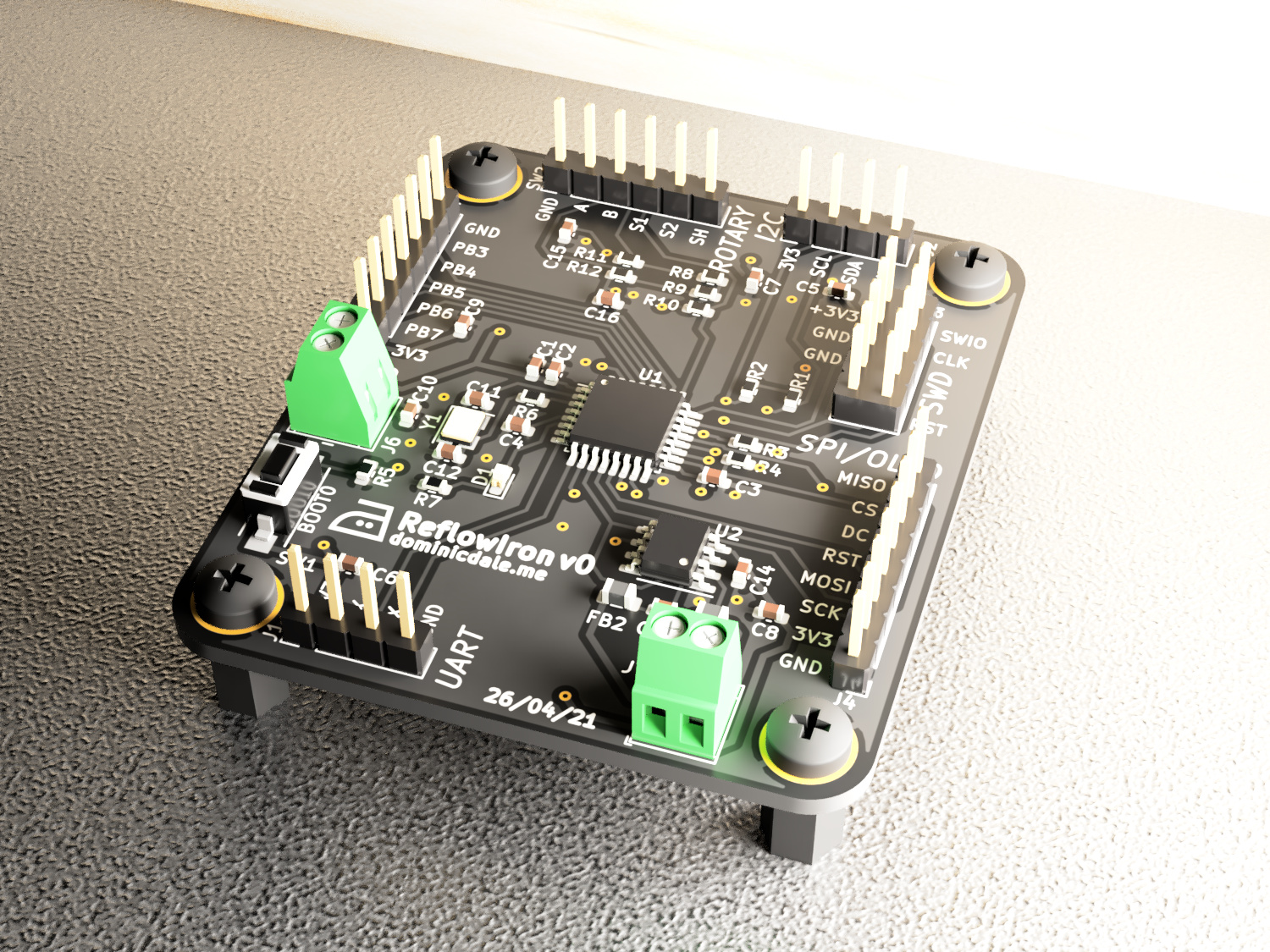
With the setup done, it’s now really easy to render multiple angles of your board with complex lighting and background capabilities. Adjusting reflectivity of the PCB materials can help achieve a glassy or more textured look.
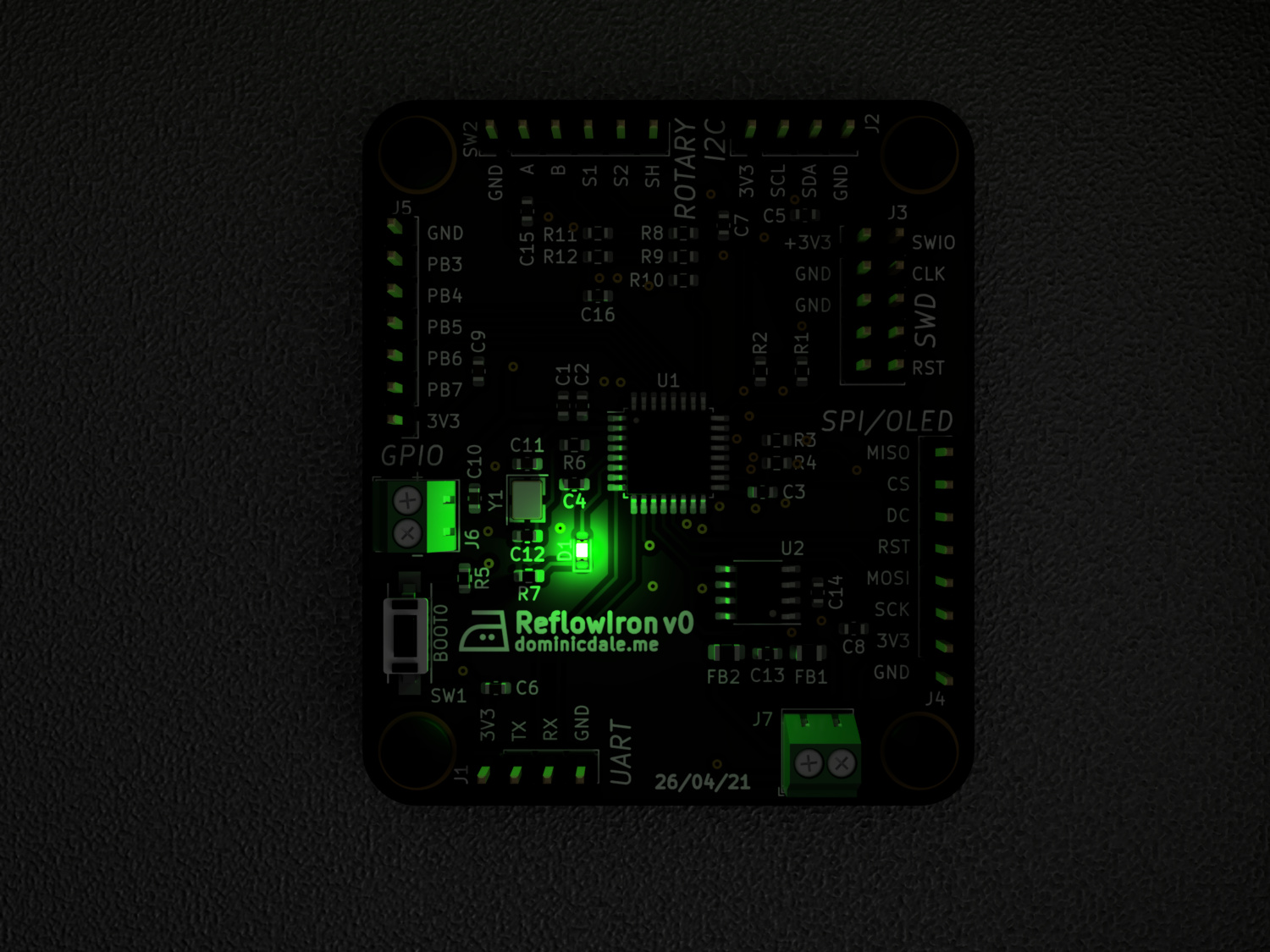
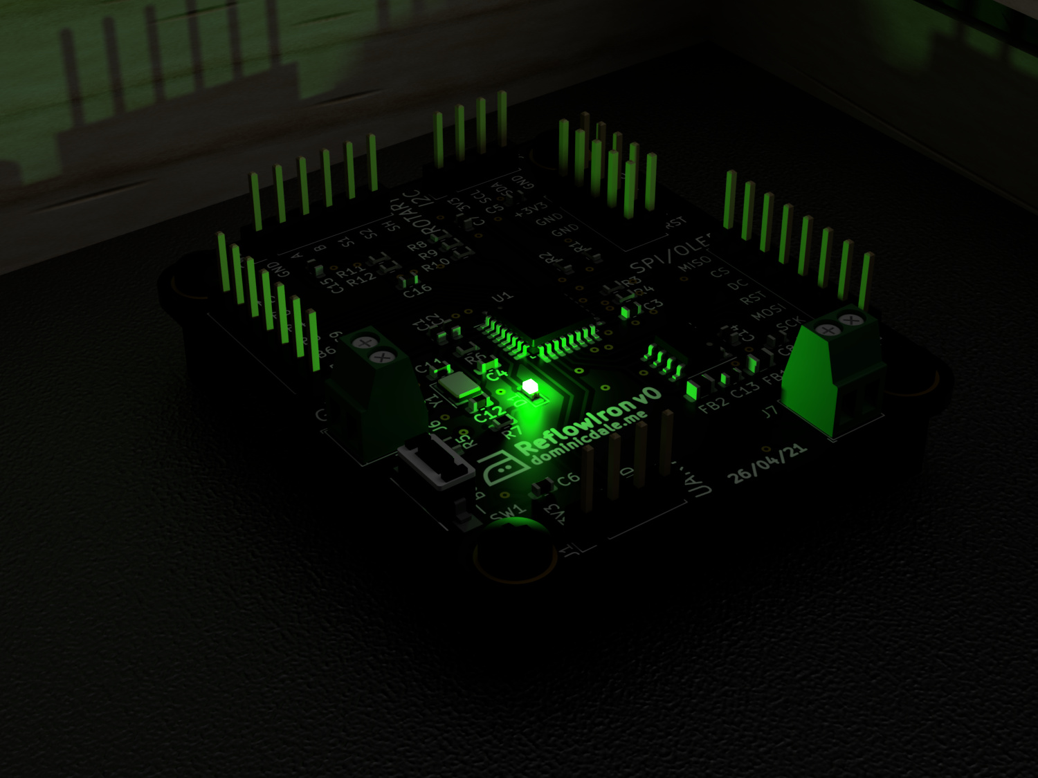
It’s possible to add luminous materials which work well for LEDs.

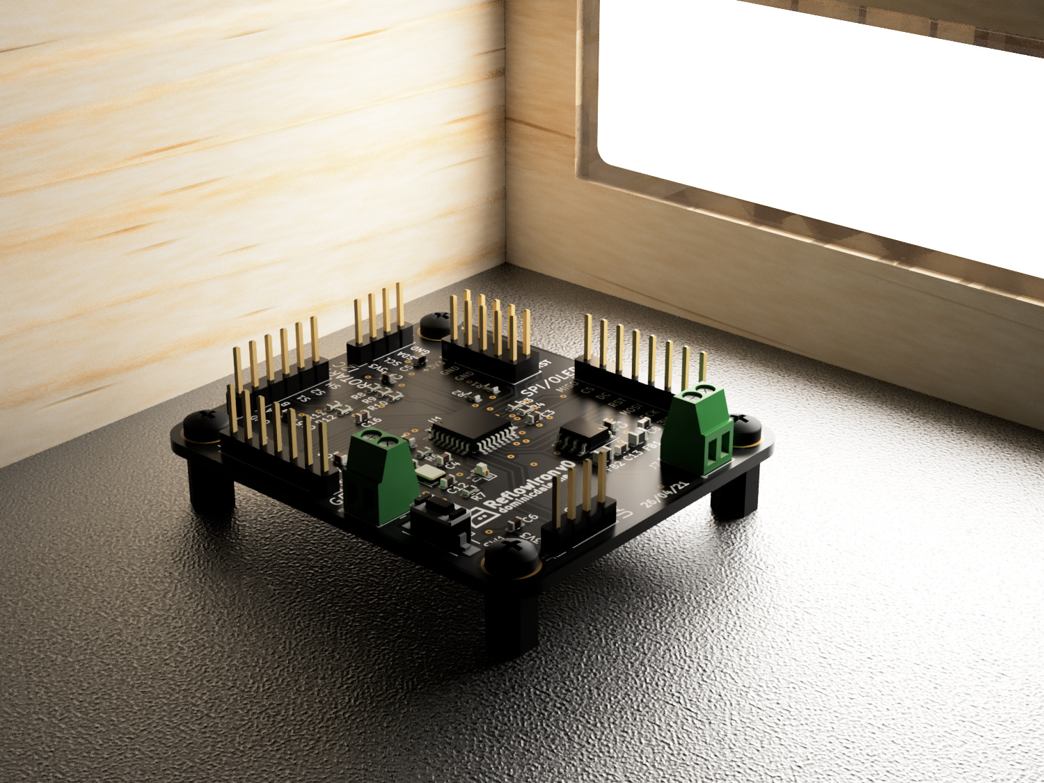
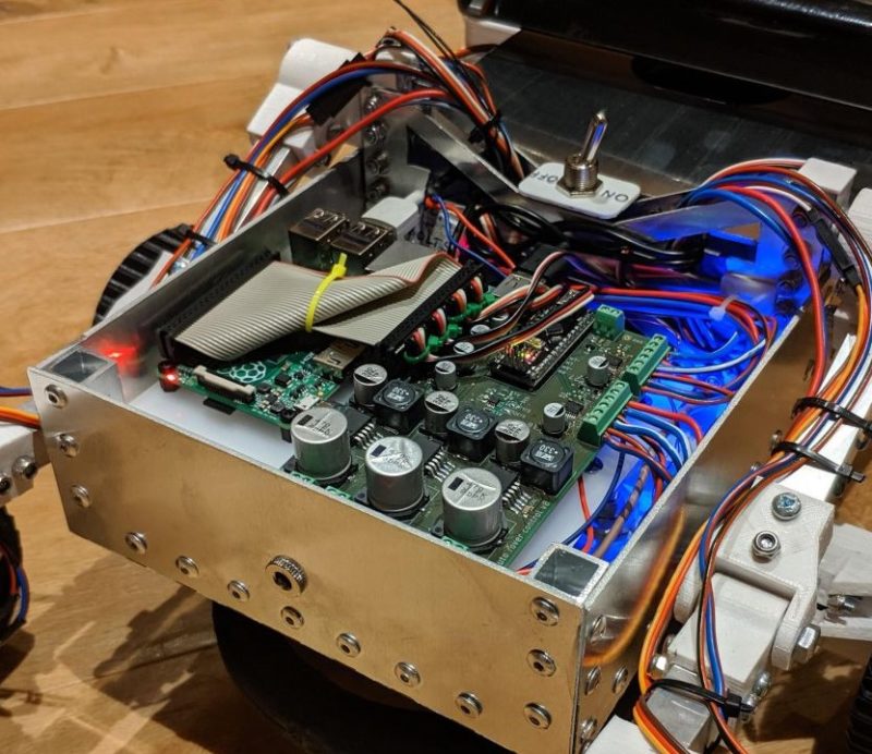
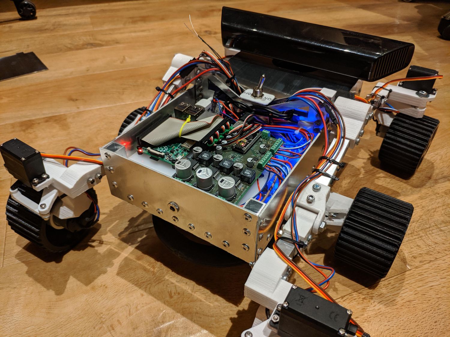
The renders aren’t just restricted to the PCB though, and the saved model can easily be dragged into a larger design (e.g. a chassis).
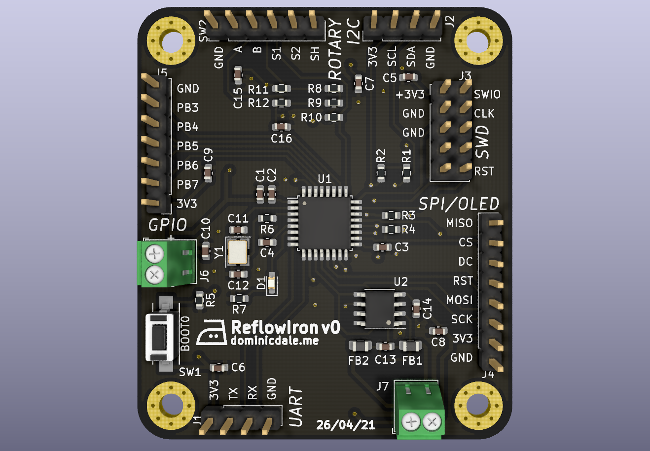
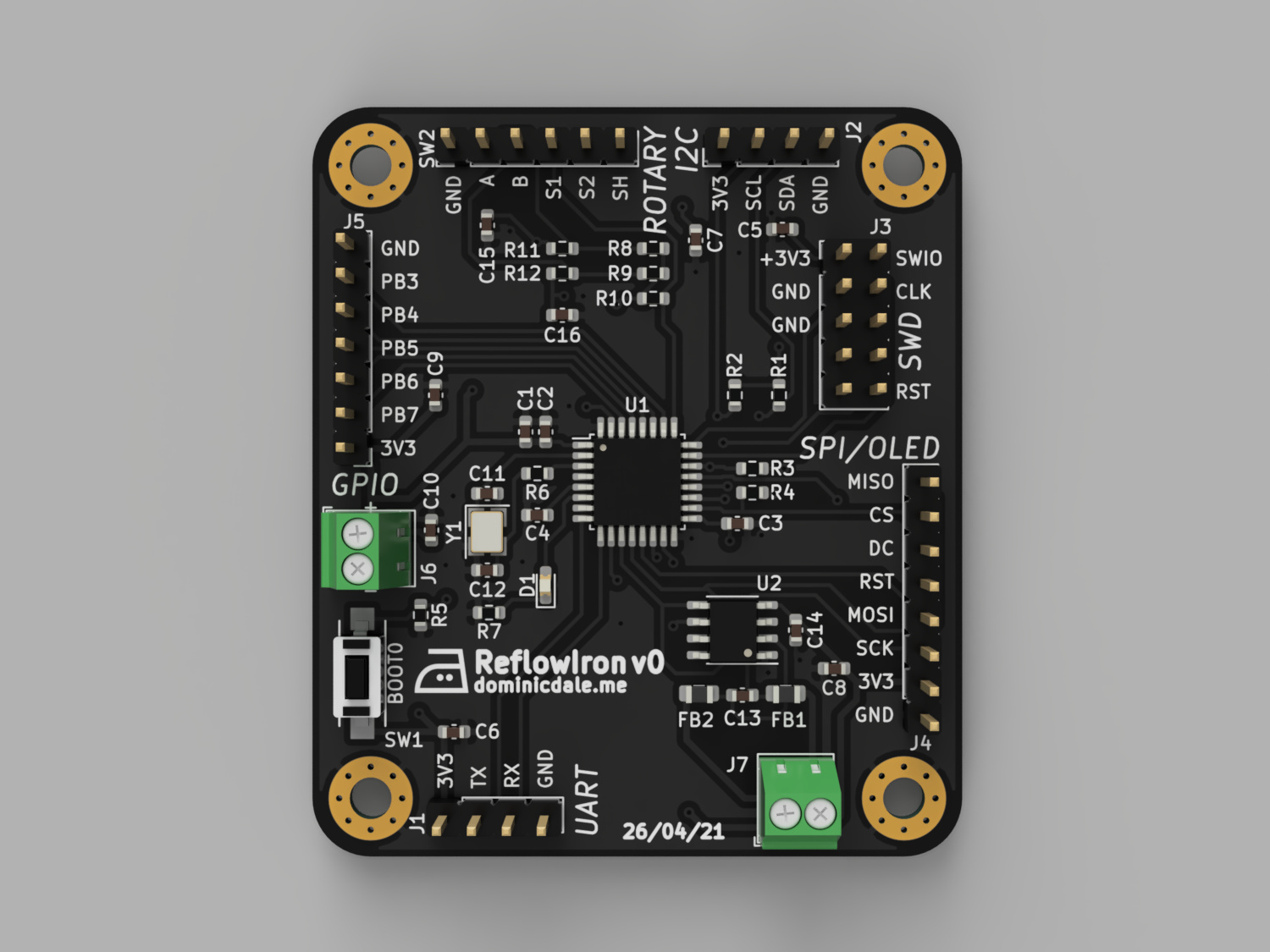
You can also create a design drawing of your model to generate a top down perspective, good for build manuals/reference material.
I’m sure with more time and tuning you could get even better results, given the power of Fusion 360’s rendering environment.